(China (Mainland))


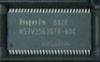
Product Summary
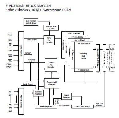
The Hynix H57V2562GTR-60C Synchronous DRAM is 268,435,456bit CMOS Synchronous DRAM, ideally suited for the consumer memory applications which requires large memory density and high bandwidth. It is organized as 4banks of 4,194,304 x 16 I/O. Synchronous DRAM is a type of DRAM which operates in synchronization with input clock. The H57V2562GTR-60C SDRAM latch each control signal at the rising edge of a basic input clock (CLK) and input/output data in synchronization with the input clock (CLK). The address lines of H57V2562GTR-60C are multiplexed with the Data Input/ Output signals on a multiplexed x16 Input/ Output bus. All the commands are latched in synchronization with the rising edge of CLK.
Parametrics
H57V2562GTR-60C absolute maximum ratings: (1)Ambient Temperature, TA: 0 to 70℃; (2)Storage Temperature, TSTG: -55 to 125℃; (3)Voltage on Any Pin relative to VSS, VIN, VOUT: -1.0 to 4.6V; (4)Voltage on VDD supply relative to VSS, VDD, VDDQ: -1.0 to 4.6V; (5)Short Circuit Output Current, IOS: 50mA; (6)Power Dissipation, PD: 1W.
Features
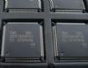
H57V2562GTR-60C features: (1)Standard SDRAM Protocol; (2)Internal 4bank operation; (3)Power Supply Voltage: VDD=3.3V, VDDQ=3.3V; (4)All device pins are compatible with LVTTL interface; (5)Low Voltage interface to reduce I/O power; (6)8,192 Refresh cycles/64ms; (7)Programmable CAS latency of 2 or 3; (8)Programmable Burst Length and Burst Type; (9)Commercial Temp : 0℃ to 70℃ Operation; (10)Package Type : 54-Pin TSOPII.
Diagrams